Gresham Fab
Atmel
SEMI-CONDUCTOR FABRICATION & SUPPORT FACILITIES
BELOW ARE DESCRIPTIONS OF EXAMPLE PROJECTS IN THIS CATEGORY
Projects that Merrick led in association or employment with other firms or agencies are identified (xxx) and keyed to the full name.
National Semiconductor Corp., Generic Fab Programming Report (JEC-96)
Project coordinator and editor for the programming report for the design of four planned 600,000 SF Fabs with 46,000 SF of Class I ballroom style cleanroom, offices, 800 seat cafeteria, conference center, and all technical support spaces. Organized around the subject areas of Function, Form, Economy, Schedule, and Organization, the report examines the requirements for transitioning to 0.18 micron geometry production, analyzes costs for providing flexibility and redundancy, and develops alternative project schedules. The Form section provides room descriptions, space tabulations, and conceptual drawings.
National Semiconductor Corp., Fab 3, Arlington, Texas (JEC-95)
Spec writer for this $57 million renovation to construct a 28,000 SF class 1 ballroom with fan tower air recirc. within an existing facility. A new central utility building and chemical storage/distribution building was added.
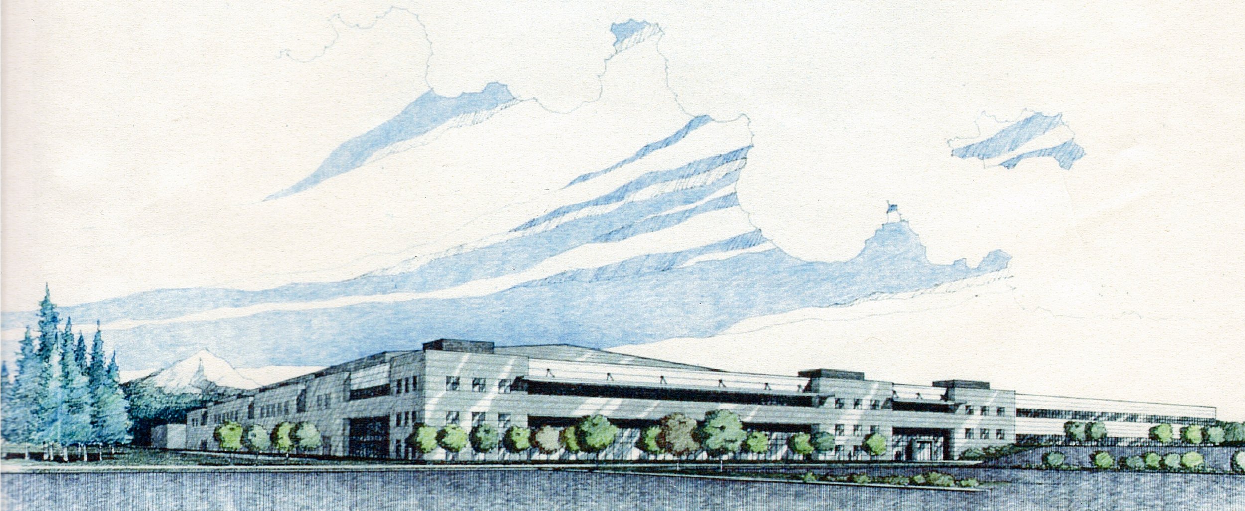
Fujitsu Microelectronics Inc., Fab 2, Gresham, OR (JEC)
Project Architect responsible for schematic design drawings and exterior and interior finishes and materials and landscape concept along with presentation documents for the design-build competition. The project consisted of a 400,000 SF manufacturing building with 90,000 SF of Class 500/10/1 cleanroom, a 140,000 SF office and support building and a 50,000 SF utility building. The setting is a landscaped campus surrounded by residential uses.
National Semi-Conductor, MOS 2 &3 Expansion, West Jordan, Utah (JEC-94)
Design manager for this $2 million remodel to relocate a clean maintenance shop and provide additional class 1 cleanroom production space. The work involved excavation and concrete work within the existing clean area. The facility required numerous life safety and exit code compliance upgrades and a new central recirc fan system.
Cypress Semiconductor, Bloomington, Minnesota (JEC-94)
Architect responsible for materials research, specifications, and building section studies for the schematic design report for a 95,000 SF addition to an existing wafer fabrication facility. Project includes 30,000 SF of Class 10/1 cleanroom and subfab with pressurized plenum fan tower air system; new chemical loading and storage areas.
Intel Fab 5 East Expansion, Intel Aloha Campus, Aloha, Oregon (JEC-94)
Architect for the remodel and 6000 SF addition to the wafer fabrication facility to accommodate the Etch Process Group and support facilities. The project was uniquely designed to be constructed without interruption to ongoing production operations. Merrick's responsibilities involved code analysis, construction drawings, and construction administration.
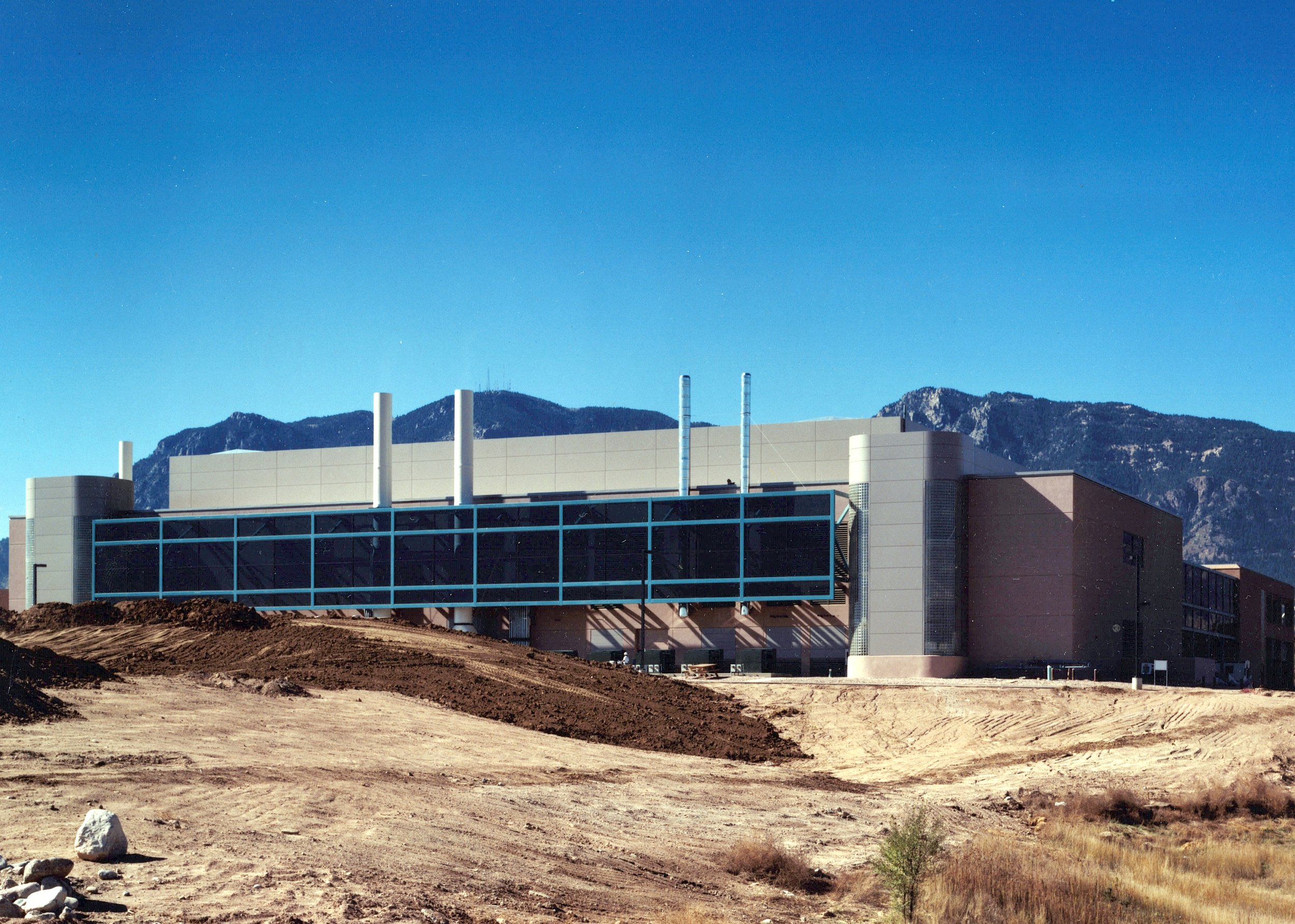
Atmel Fab 5 Atmel Corporation, Colorado Springs, Colorado (JEC-93)
Project Architect for the design of the new 175,000 SF wafer fabrication facility with capacity for 40,000 SF of Class 10 cleanroom. The compressed fast-track schedule was completed under a design and construction management contract. Responsibilities included space needs programming, site analysis, code analysis, coordinating design for the building shell, service yards, utility systems, site landscaping and civil work, design development and construction documents for the shell and spill containment measures for RO/DI and for hazardous chemical delivery and storage areas. The project was completed and operational within 16 months of inception.